- 您现在的位置:买卖IC网 > Sheet目录697 > OP4010B (RFM)IC OPT TIME CLK 663.552MHZ 8-SMC
�� �
�
�OP4010B�
�?�
�Quartz� SAW� Stabilized� and� Filtered� “Diff� Sine”� Technology�
�?�
�?�
�?�
�Fundamental-Mode� Oscillation� at� 663.552� MHz�
�Voltage� Tunable� for� Phase� Lock� Loop� Operations�
�Optical� Timing� Reference� for� Forward� Error� Correction� Applications�
�663.552� MHz�
�Optical�
�The� output� of� this� device� is� generated� and� filtered� by� narrowband� quartz� SAW� elements� at� 663.552� MHz.� The�
�configuration� of� this� clock� is� intended� to� provide� a� pure� signal� for� optical� timing� applications� in� noisy� signal�
�environments.� The� Q/Qbar� differential� output� swing� of� ±1� volt� about� 0� vdc� has� symmetry� better� than� ±1%� into�
�loads� from� 40� ohms� to� 70� ohms;� determined� by� customer� application.� The� long� term� frequency� accuracy� is�
�set� by� an� external� reference� source� allowing� this� device� to� complete� a� Phase� Lock� Loop� design� without� the�
�usual� noise� and� jitter� problems� associated� with� PLL’s.�
�Absolute� Maximum� Ratings�
�Timing� Clock�
�Rating�
�DC� Suppy� Voltage�
�Tune� Voltage�
�Value�
�0� to� 5.5�
�0� to� 6�
�Units�
�VDC�
�VDC�
�Case� Temperature�
�-55� to� 100�
�°C�
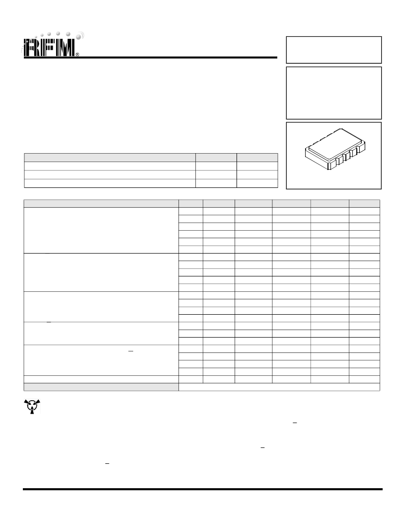
�SMC-08�
�Electrical� Characteristics�
�Characteristic�
�Operating� Frequency�
�Absolute� Frequency�
�Sym�
�f� O�
�Notes�
�1,� 9�
�Minimum�
�Typical�
�663.552�
�Maximum�
�Units�
�MHz�
�Tune� Range�
�2�
�±100�
�ppm�
�Tune� Voltage�
�Tuning� Linearity�
�1�
�1,� 8�
�0�
�±3%�
�+3�
�VDC�
�Tuning� Sensitivity�
�df/dv�
�2,� 10�
�140�
�300�
�ppm/V�
�Modulation� Bandwidth�
�50�
�kHz�
�Q� and� Q� Output�
�Voltage� into� 50� Ω� (VSWR� ≤� 1.2)�
�V� O�
�1,3�
�0.60�
�1.1�
�V� P-P�
�Operating� Load� VSWR�
�1,3�
�2:1�
�Phase� Noise�
�Symmetry�
�Harmonic� Spurious�
�Nonharmonic� Spurious�
�dBc/Hz@100Hz� offset�
�1kHz� offset�
�3,� 4,� 5�
�3,� 4,� 6�
�3,� 4,� 6,� 7�
�49�
�-75�
�-105�
�51�
�-30�
�-60�
�%�
�dBc�
�dBc�
�dBc/Hz�
�dBc/Hz�
�10k� offset�
�Noise� Floor�
�-125�
�-155�
�Q� and� Q� Jitter�
�RMS� Jitter�
�No� Noise� on� V� CC�
�200� mV� P-P� from� 1MHz� to� ?� f� O� on�
�3,� 4,� 6,� 7�
�3,� 4,� 6,� 7�
�3�
�2�
�12�
�12�
�PS� P-P�
�PS� P-P�
�PS� P-P�
�Input� Impedence� (Tuning� Port)�
�1�
�K� Ω�
�Output� DC� Resistance� (between� Q� &� Q)�
�1,� 3�
�50�
�K� Ω�
�DC� Power� Supply�
�Operating� Voltage�
�V� CC�
�1,� 3�
�3.13�
�3.3,� 5.0�
�5.25�
�VDC�
�Operating� Current�
�I� CC�
�1,� 3�
�70�
�mA�
�Operating� Case� Temperature�
�T� C�
�1,� 3�
�-40°C�
�+85°C�
�°C�
�Lid� Symbolization� (YY=Year,� WW=Week)�
�RFM� OP4010B� YYWW�
�CAUTION:� Electrostatic� Sensitive� Device.� Observe� precautions� for� handling.�
�COCOM� CAUTION:� Approval� by� the� U.S.� Department� of� Commerce� is� required� prior� to� export� of� this� device.�
�Notes:�
�1.�
�2.�
�3.�
�4.�
�5.�
�6.�
�7.�
�8.�
�9.�
�Unless� otherwise� noted,� all� specifications� include� any� combination� of� load� VSWR,� Vcc,� and� temperature,� with� Q� and� Q� terminated� into� 50� ohm� loads� to�
�ground� (see� typical� test� circuit).�
�Useful� tuning� range� is� in� excess� of� what� is� required� over� temp,� aging,� pushing,� pulling� &� accuracy.�
�The� design,� manufacturing� process,� and� specifications� of� this� device� are� subject� to� change� without� notice.�
�Only� under� the� nominal� conditions� of� 50� Ω� load� impedance� with� VSWR� ≤� 1.2� and� nominal� power� supply� voltage.�
�Symmetry� is� defined� as� the� pulse� width� (in� percent� of� total� period)� measured� at� the� 50%� points� of� Q� or� Q� (see� timing� definitions).�
�Jitter� and� other� spurious� outputs� induced� by� externally� generated� electrical� noise� on� V� CC� or� mechanical� vibration� are� not� included� in� this� specification,� except�
�where� noted.� External� voltage� regulation� and� careful� PCB� layout� are� recommended� for� optimum� performance.�
�Applies� to� period� jitter� of� Q� and� Q.� Measurements� are� made� with� the� Tektronix� CSA803� signal� analyzer� with� at� least� 1000� samples.�
�Linearity� is� a� function� of� the� percentage� variation� from� a� permitted� linear� deviation� versus� the� amount� of� frequency� tune� range� (see� linearity� definition).�
�One� or� more� of� the� following� United� States� patents� apply:� 4,616,197;� 4,670,681;� 4,760,352.�
�www.RFM.com� E-mail:� info@rfm.com�
�?2008� by� RF� Monolithics,� Inc.�
�Page� 1� of� 2�
�OP4010B� -� 3/27/08�
�发布紧急采购,3分钟左右您将得到回复。
相关PDF资料
OP4011B
IC OPT TIME CLK 719.734MHZ 8-SMC
OP4012B
IC OPT TIMECLK 644.53125MHZ 8SMC
OP4013B
IC OPT TIMECLK 693.48342MHZ 8SMC
OP4014B
IC OPT TIME CLK 627.329MHZ 8-SMC
OP4015B
IC OPT TIME CLK 780.881MHZ 8-SMC
ORD211-2030
SWITCH REED SPST-NO 10MM OKI
ORD213S-1T-1015
REED SWITCH 24VDC 1W SMD TR
ORD219-1015
SWITCH REED SPST-NO 12MM OKI
相关代理商/技术参数
OP4011B
功能描述:IC OPT TIME CLK 719.734MHZ 8-SMC RoHS:是 类别:晶体和振荡器 >> 振荡器 系列:- 标准包装:1 系列:VG-4512CA 类型:VCXO 频率:153.6MHz 功能:三态(输出启用) 输出:LVPECL 电源电压:3.3V 频率稳定性:- 工作温度:-40°C ~ 85°C 电流 - 电源(最大):60mA 额定值:- 安装类型:表面贴装 尺寸/尺寸:0.276" L x 0.197" W(7.00mm x 5.00mm) 高度:0.071"(1.80mm) 封装/外壳:6-SMD,无引线(DFN,LCC) 包装:Digi-Reel® 电流 - 电源(禁用)(最大):- 其它名称:SER3790DKR
OP4012B
功能描述:IC OPT TIMECLK 644.53125MHZ 8SMC RoHS:是 类别:晶体和振荡器 >> 振荡器 系列:- 标准包装:1 系列:VG-4512CA 类型:VCXO 频率:153.6MHz 功能:三态(输出启用) 输出:LVPECL 电源电压:3.3V 频率稳定性:- 工作温度:-40°C ~ 85°C 电流 - 电源(最大):60mA 额定值:- 安装类型:表面贴装 尺寸/尺寸:0.276" L x 0.197" W(7.00mm x 5.00mm) 高度:0.071"(1.80mm) 封装/外壳:6-SMD,无引线(DFN,LCC) 包装:Digi-Reel® 电流 - 电源(禁用)(最大):- 其它名称:SER3790DKR
OP4013B
功能描述:IC OPT TIMECLK 693.48342MHZ 8SMC RoHS:是 类别:晶体和振荡器 >> 振荡器 系列:- 标准包装:1 系列:VG-4512CA 类型:VCXO 频率:153.6MHz 功能:三态(输出启用) 输出:LVPECL 电源电压:3.3V 频率稳定性:- 工作温度:-40°C ~ 85°C 电流 - 电源(最大):60mA 额定值:- 安装类型:表面贴装 尺寸/尺寸:0.276" L x 0.197" W(7.00mm x 5.00mm) 高度:0.071"(1.80mm) 封装/外壳:6-SMD,无引线(DFN,LCC) 包装:Digi-Reel® 电流 - 电源(禁用)(最大):- 其它名称:SER3790DKR
OP4014B
功能描述:IC OPT TIME CLK 627.329MHZ 8-SMC RoHS:是 类别:晶体和振荡器 >> 振荡器 系列:- 标准包装:1 系列:VG-4512CA 类型:VCXO 频率:153.6MHz 功能:三态(输出启用) 输出:LVPECL 电源电压:3.3V 频率稳定性:- 工作温度:-40°C ~ 85°C 电流 - 电源(最大):60mA 额定值:- 安装类型:表面贴装 尺寸/尺寸:0.276" L x 0.197" W(7.00mm x 5.00mm) 高度:0.071"(1.80mm) 封装/外壳:6-SMD,无引线(DFN,LCC) 包装:Digi-Reel® 电流 - 电源(禁用)(最大):- 其它名称:SER3790DKR
OP4015B
功能描述:IC OPT TIME CLK 780.881MHZ 8-SMC RoHS:是 类别:晶体和振荡器 >> 振荡器 系列:- 标准包装:1 系列:VG-4512CA 类型:VCXO 频率:153.6MHz 功能:三态(输出启用) 输出:LVPECL 电源电压:3.3V 频率稳定性:- 工作温度:-40°C ~ 85°C 电流 - 电源(最大):60mA 额定值:- 安装类型:表面贴装 尺寸/尺寸:0.276" L x 0.197" W(7.00mm x 5.00mm) 高度:0.071"(1.80mm) 封装/外壳:6-SMD,无引线(DFN,LCC) 包装:Digi-Reel® 电流 - 电源(禁用)(最大):- 其它名称:SER3790DKR
OP402-905
制造商:TT Electronics / OPTEK Technology 功能描述:
OP41
制造商:AD 制造商全称:Analog Devices 功能描述:LOW-BIAS-CURRENT, HIGH-STABILITY JFET OPERATIONAL AMPLIFIER
OP-41
制造商:AD 制造商全称:Analog Devices 功能描述:LOW-BIAS-CURRENT, HIGH-STABILITY JFET OPERATIONAL AMPLIFIER